Power Factor Correction Rectifier Based on Boost Converters Using Negative Slope Ramp Carrier Control Technique
T. Tanitteerapan
Abstract -- This paper, power factor correction rectifier based on boost converters using the negative slope ramp carrier control technique. The duty ratio is obtained by the comparison of a sensed signal from inductor current and a negative slope ramp carrier waveform in each switching period. Because the negative slope ramp carrier controller requires only the inductor current sensor and the output voltage sensor, its control circuit implementation is very simple. To verify the controller design, the circuit experimentation of a 150 W boost AC-DC converter with the negative slope ramp carrier controller was applied. As the result, the input current waveform was shaped to be closely sinusoidal, implying high power factor.
Index Terms —Power Factor Correction, High Power Factor Rectifier, Continuous Conduction Mode Control, Current Mode Control.
Introduction
Boost converter is one of the most popular choices for using as the power factor correction (PFC) converter. The converter is supplied from a full wave rectified line voltage and operated so that the input current follows the input voltage. The input current waveshaping can be achieved using a number of techniques. When the converter is operated at fixed frequency and fixed duty ratio in the discontinuous conduction mode (DCM), the low frequency component of the input current is approximately proportional to the input voltage, so that the power is automatically close to one [1]. However, the DCM operation causes a large current stress on semiconductors and demands more effort to attenuate the current ripple so as to have a satisfactory low electromagnetic interference (EMI) to the line. Therefore, in medium and high power applications, the continuous conduction mode (CCM) is preferred because the current stress and current ripple become too large when operating the converter in the DCM. Traditionally, to operate the boost AC-DC converter in the CCM, the conventional controller in [2] is applied. However, its control circuit implementation is very complex. A number of papers have been dedicated to simplify the complexity of conventional control circuit implementation [3]-[7]. These papers eliminated the multiplier, the input voltage sensor, and the error amplifier in the current control loop. Some method fulfilled that purpose under the penalty of higher current distortion [3]. The nonlinear-carrier (NLC) control proposed in [4] is one of good example for the simple CCM operation control technique. The sinusoidal switch current is sensed to compare with the nonlinear carrier waveform in each switching period for achieve the sinusoidal input current waveshape or high power factor condition. The input line voltage sensor, the multiplier, and the error amplifier in the current control loop of the conventional control technique in [2] are not required in the NLC controller.
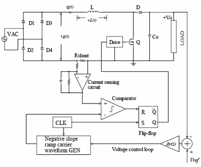
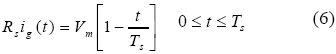
Fig. 1. Boost rectifier with negative slope ramp carrier (NSRC) control technique.
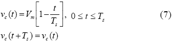
The purpose of this paper is to present a negative slope ramp carrier control technique in the CCM operation for the power factor correction rectifier based on boost converters as shown in Fig.2. The proposed controller uses the basic principle like as the principle used in the NLC controller in [4] that the duty ratio is obtained by the comparison of the sensed current and the parabolic carrier waveform in each switching period. However, the proposed controller does not use the integrator circuit of the sensed current as used in the NLC controller and uses the negative slope ramp carrier waveform, which has the generator circuit implementation simpler than the NLC controller. The proposed controller obtains the duty ratio in each switching period from the comparison of the negative ramp carrier waveform vc(t) and the sensed inductor current signal Rsig(t). So, the input voltage sensor, the error amplifier in the current control mode Ai(s), and the multiplier as used in the conventional control technique are not required. The design consideration of the proposed controller is expressed in section II. In section III, small signal AC frequency modeling for the boost rectifier with the negative slope ramp carrier control technique are explained. Section VI shows the experimental verification of a 150W boost rectifier with the proposed controller.
Design consideration of the negative slope ramp carrier control technique
The boost rectifier as shown in Fig.1 is well-known switched-mode converter that is capable of producing a dc output voltage greater than the input voltage that can be determined from

where vg(t) is the input voltage, d(t) is the duty ratio and vo(t) is the output voltage.
When the unity power factor condition occurs, the converter looks like a resistor, which is called as the emulated resistor Re. The Re is determined by
where ig(t) is the input current.
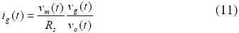
Therefore, the input current ig(t) can be yielded from
where the output voltage is the small-ripple approximation so that vo(t)  vo. vo.
Equation (3) is the relation of the current form that in practical design, to realize the relation in equation (3) to implement the proposed control circuit, the relation of the voltage form is required. So, the sensing circuit resistor Rs is defined and added to equation (3) and the new relation can be yielded as
where Rs is the sensing circuit resistor.
To obtain a duty d(t) to satisfy equation (4), the signal Rsig(t) is compared with the periodic carrier waveform vc(t) which is realized by substituting d(t) with t/Ts in eqation (4) so that,

or
where Vm is the control signal from the error amplifier in the voltgae feedback loop Av(s). Then, the negative slope ramp carrier waveform vc(t) can be obtained by
By using equations (4) and (6), the emulated resistance Re can be determined by
Small signal ac frequency modeling for the boost converter with the negative slope ramp carrier controller
The ac frequency modeling of the boost AC-DC converter with the proposed controller for the error amplifier of the voltage control mode Av(s) (the output voltage regulating loop) is designed based on the stabilization of the converter output voltage against variations in load power, ac line voltage, and component characteristics. The voltage regulating loop cannot attempt to remove the capacitor voltage ripple that occurs at the second harmonic of the ac line frequency, 2 , since doing so would require that Re changes significantly at the second harmonic frequency. Therefore, this loop must have sufficiently small gain at frequency 2 and its bandwidth must be low. To design the small signal ac frequency modeling, equations (4), (5), and (6) are used to be considered and here we define that the control signal vm(t) is varied with time at the second harmonic of ac line frequency 2 so that the new relation can be re-written as. , since doing so would require that Re changes significantly at the second harmonic frequency. Therefore, this loop must have sufficiently small gain at frequency 2 and its bandwidth must be low. To design the small signal ac frequency modeling, equations (4), (5), and (6) are used to be considered and here we define that the control signal vm(t) is varied with time at the second harmonic of ac line frequency 2 so that the new relation can be re-written as.

then,
Using the relation of the emulated resistor Re in equation (8) to substitute in equation (10),
the input current ig(t) can be yielded by
where the output voltage vo(t) is varied with time at the second harmonic of ac line frequency 2.
Based on the power balance on a 2 or 100 Hz time scale, the relation of the power input and the power output of the AC-DC converter can be yielded by

where Vg,rms is the root mean square value of the input voltage, Ig,rms is the root mean square value of the input current and here, we assume that no any loss occurs in the converter.
The relation depending on time of equation (12) can be written as

Substituting equation (11) to equation (13), then the new relation can be yielded as
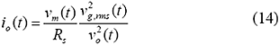
where io(t) is the output current.
Linearize equation (14) so that
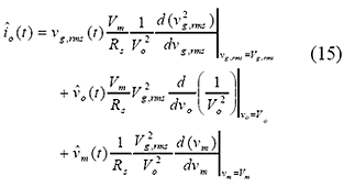
where is the small signal of the output current io(t).
Then,
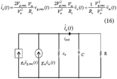
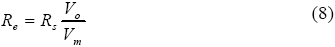
Fig. 3. Small signal ac frequency modeling of the boost AC-DC converter with the proposed controller (where Co = the output capacitor of the boost converter and R is the output resistor of the boost converter).
Here, we define the notation of the small signal ac frequency modeling of the boost rectifier with the proposed controller from equation (16) as,
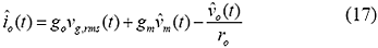
where the parameter values are given by
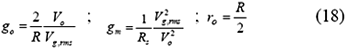
By using the relation in equations (17) and (18), the small signal ac frequency modeling circuit for designing the error amplifier of the output voltage regulating loop can be shown in Fig.3.
Experimental Verifications
To verify the proposed controller that use to control the boost converter as the AC-DC converter, the circuit experimentation was applied by designing to meet the following specifications:
the output power Po = 150 W, the output voltage Vo = 380 Vdc, the input voltage Vg,rms = 100 Vrms, the line frequency f = 50 Hz, the switching frequency fs = 40 kHz, Inductance (L) = 2 mH, and the load resistance R at full load is equal to 950  . .
From the small signal ac frequency modeling in Fig.3, the transfer function F(s) of the boost AC-DC converter with the proposed controller can be yielded as
Here, the converter pole frequency is defined as p = 3 / RCo
Therefore, the voltage regulating control loop gain T(s) can be determined from

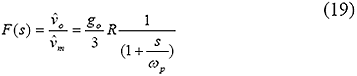
We define the transfer function of the error amplifier of the voltage control mode Av(s) as
where o is the amplifier frequency, z1 is the compensator zero frequency No.1, and z2 is the compensator zero frequency No.2. Then, equation (20) can be re-written as
where H(s) is the output voltage sensor gain.
Equation (22) is used to implement the output voltage regulator, which has the circuit parameters as shown in the experimental circuit in Fig.4
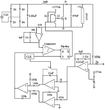
Fig. 4. Experimental circuit of the 150W boost AC-DC converter with the negative slope ramp carrier controller.
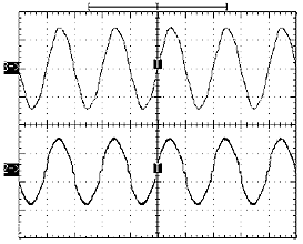
Fig. 5 Experimental waveforms of (topper) input voltage [100V/div], and (lower) input current [2A/div].
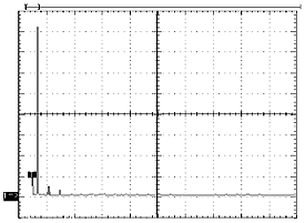
Fig. 6 Spectrum of the input current waveform in Fig.5.
By using the circuit operation in Fig.4, the input current waveform (shown in Fig.5 lower trace) is shaped to be closely
sinusoidal by following the input voltage waveform (shown in Fig.5 toper trace). Fig.6 shows the spectrum of input current waveform, which shows in Fig.5. The total harmonic distortion (THD) at loads during 10-100% are shown in Fig.7. The THD is about 5% at full load condition and although the converter operates in the DCM, the THD is not exceeded 15%.
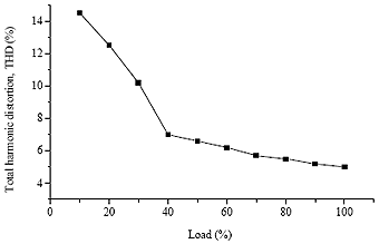
Fig. 7 Total harmonic distortion (THD) versus load
Conclusion
The power factor correction rectifier based on boost converters using negative slope ramp carrier control technique in CCM operation was introduced and verified by the experimentation of 150W boost rectifier. The proposed controller requires only the output voltage and inductor current sensors. So, the error amplifier in the current control mode, the input voltage sensor, and the multiplier used in the conventional controller are not required. The duty ratio is determined by comparing the sensed peak inductor current with the negative slope ramp carrier waveform in each switching period. By using the proposed controller, the input current waveform of boost AC-DC converter was shaped to be closely sinusoidal by following the input voltage waveform.
References
D. Chambers and D. Wang, “ Dynamic P.F. correction in capacitor input off-line converters,” in Proc. Powercon 6, Miami Beach, FL, May 2-4, 1979, pp, B3.1-6.
M. Kazerani, P.D.Ziogas and G.Joos, “A novel active current waveshaping technique for solid-state input power factor conditioners,” IEEE Trans. Industry Electronics, vol.38, no.1, February 1991.
D. Maksimovic, “Design of clamped-current high-power-factor boost rectifiers,” Applied Power Electronics Conference and Exposition, 1994. APEC '94 Conference Proceeding 1994, pp. 548-590.
D. Maksimovic, Yungtaek Jang, and Robert W. Erickson “Nonlinear-Carrier Control for High Power Factor Boost Rectifiers,” IEEE Trans. Power Electronics, vol. 11, No. 4, March 1996, pp. 578-584.
J. R Gegner, C. Q. Lee, “Linear Peak Current Mode Control: A Simple Active Power Factor Correction Control Technique for Continuous Conduction Mode,” Power Electronics Speasialist Conference., 1996, PESC’96 Conference Proceedings 1996, pp. 196-202.
J. Hwang, A. Chee and W. H. Ki “New Universal Control Methods for Power factor Correction and DC to DC Converter Application,” Applied Power Electronics Conference and Exposition, 1997. APEC '97 Conference Proceedings 1997, Twelfth Annual, Volume: 1, 1997 Page(s): 59 -65 vol.1.
Z.Lai and K.M. Smedley, “A family of continuous conduction mode power factor correction controller based on the general pulse width modulator,” IEEE Tran. Power Electronics, vol.13, no.3, May 1998.
|